
The iC‑MU200 evaluation system, provided by IC‑HAUS, offers a straightforward way to test and characterise the device. This guide walks through the setup using the iC‑MU200 as an example. The test platform is designed to let you evaluate the absolute magnetic encoder’s functionality, configure its registers, and perform electrical calibration via the official PC‑based GUI software. The complete system consists of three hardware layers, connected in a “daughter‑board → motherboard → adapter” chain:
- Sensor Daughter Board:
iC‑MU200 EVAL MU6M– carries the main encoder IC.
- Sensor Daughter Board:
- Motherboard Expansion:
iC‑MU EVAL MU1D– breaks out all electrical interfaces.
- Motherboard Expansion:
- USB Adapter:
iC‑MB3 iCSY MB3U‑I2C– bridges the motherboard to a PC.
- USB Adapter:
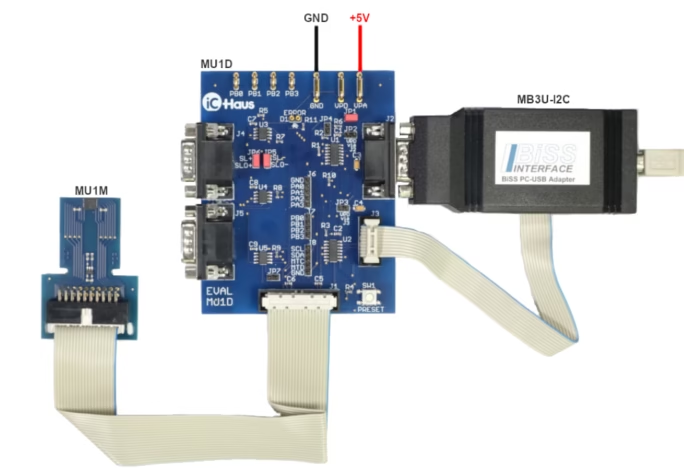
1. Hardware Component Details
A. iC‑MU200 EVAL MU6M Sensor Daughter Board
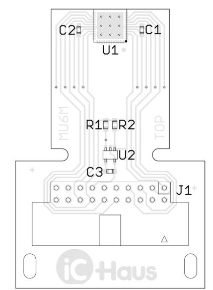
- Core IC: The board hosts an iC‑MU200 in a QFN48 package, whose internal Hall sensors are optimised for a 2.0 mm master‑track pole width.
- External EEPROM: A 16 kbit 24LC16B (SOT‑23) stores configuration parameters that load at power‑up.
- Connector: The
J1(2×10‑pin right‑angle header) routes all key I/O, power, multi‑turn, and I²C signals to the motherboard.
- Connector: The
- Default Configuration: Factory‑programmed settings enable the SPI interface and support a 32/31 pole‑pair differential nonius disc (e.g., MU37S 45‑32N).
B. iC‑MU EVAL MU1D Motherboard Expansion
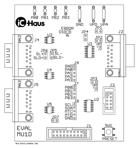
- Function: Acts as the physical hub. It converts the fine‑pitch signals from the daughter board into standard test points and connectors, and includes necessary drive/buffer circuitry.
- Key Connectors and Headers:
J1(20‑pin socket) – connects to the daughter board’sJ1via a 20‑pin ribbon cable.
J2(9‑pin D‑sub female) – for a PC adapter that supports BiSS/SSI.
J3(10‑pin WSL box header) – for a PC adapter supporting SPI.
J5(9‑pin D‑sub male) – multi‑turn interface for daisy‑chaining external encoder ICs in multi‑turn systems.
J6,J7,J8(test pins) – allow oscilloscope probes to monitor Port A, Port B, I²C bus, and multi‑turn timing signals.
- Key Connectors and Headers:
- Jumper Settings:
- JP1 (closed by default) – bridges analog (VPA) and digital (VPD) supplies; open to measure or supply them separately.
- JP2 & JP3 – enable or disable VDD power from the adapter connected to J2 (BiSS) or J3 (SPI).
- JP4 – when closed, disables the Port A I/O buffer. Must be closed when using the SPI interface (J3) to avoid bus contention.
- JP5/JP6 – BiSS loop selection. Closed for point‑to‑point loopback; open for daisy‑chain configurations.
- JP7 – disconnects the MAX3087 differential transceiver on the MTD line when differential drive is not needed.
- Jumper Settings:
- Push‑button SW1 – pulls the
PA0pin low on the iC‑MU200, used to force mode selection at start‑up.
- Push‑button SW1 – pulls the
C. iC‑MB3 iCSY MB3U‑I2C USB Adapter
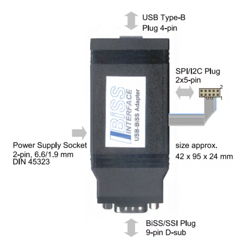
- Function: Provides bidirectional communication between the PC software and the test motherboard.
- Interface Capabilities:
- RS‑422 (J2 side): Galvanically isolated differential interface via 9‑pin D‑sub, supporting 10 MHz BiSS and 4 MHz SSI.
- Single‑ended (SPI/I²C): Master interface via 2×5 header, supporting 6 MHz SPI and 100 kHz I²C.
- Interface Capabilities:
- Power Supply: Delivers up to 200 mA at 5 V from the USB port to power the sensor.
- Compatibility Notes:
- Register and EEPROM read/write operations are supported under both SPI and BiSS modes.
- System calibration is only supported in SPI mode. The MB3U‑I2C does not support calibration over BiSS.
- Compatibility Notes:
2. System Assembly and Connection Steps
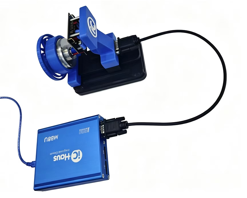
- Connect the USB adapter to the PC using a Type‑A to Type‑B USB cable.
- Link the daughter board to the motherboard – use a 20‑pin ribbon cable to connect
J1on the MU6M toJ1on the MU1D.
- Link the daughter board to the motherboard – use a 20‑pin ribbon cable to connect
- For initial SPI evaluation (recommended for first‑time power‑up and calibration):
- Close jumper JP3 on the MU1D to allow the adapter to supply power to the system.
- Close jumper JP4 to disable the Port A buffer.
- Connect the 10‑pin single‑ended header of the MB3U‑I2C to J3 on the MU1D using the 10‑pin ribbon cable.
- For initial SPI evaluation (recommended for first‑time power‑up and calibration):
3. Switching from SPI to BiSS Communication
The MU6M is factory‑set to enable SPI by default. If you later need to connect a BiSS‑only adapter (such as the MB5U) for testing or calibration, you can force the configuration using the following hardware‑based procedure:
- Power down the system.
- Short the
SDAline (on theJ8test header of the MU1D) to GND using a jumper or test lead. This prevents the chip from reading the EEPROM at next power‑up.
- Short the
- Press and hold the SW1 button on the MU1D (pulls
PA0low, signalling the chip to use BiSS mode at start‑up).
- Press and hold the SW1 button on the MU1D (pulls
- Apply USB power to turn on the system.
- Release SW1 and remove the
SDA‑to‑GND short.
- Release SW1 and remove the
- Open the
iC‑MU Series GUIsoftware on your PC, connect to the chip, and click “Write EEPROM” to store the configuration permanently.
- Open the
- Perform a
SOFT_RESET– the iC‑MU200 will now automatically start in BiSS absolute mode on every subsequent power‑up.
- Perform a
 Practical Tip
 Practical Tip
The iC‑MU200’s larger package demands tighter mechanical tolerances – a typical air gap of around 0.4 mm and careful radial runout control are essential. After establishing stable communication, always perform a full electrical self‑calibration (including phase, amplitude, and SPON track offset) using the matching magnetic disc. This prevents common signal errors such as NON_CTR (nonius synchronisation failure) during operation.
Complete Sensing Solutions from OTV Sensing
 Complete Sensing Solutions from OTV Sensing
Once you’ve validated the chip, you’ll need a reliable magnetic target to achieve high‑accuracy angle detection. OTV Sensing offers a complete ecosystem covering the entire signal chain – from evaluation hardware to custom magnetic rings:
- Precision Magnetic Rings: Standard products compatible with iC‑MU, iC‑MU150, and iC‑MU200, plus customisation options (pole‑pair count, inner/outer diameter, thickness, magnetisation pattern, etc.).
- Evaluation Kits: Ready‑to‑use packages including sensor daughter board, motherboard, and USB adapter to get you started quickly.
- Application Engineering Support: Leveraging our deep knowledge of iC‑Haus encoders and magnetic ring matching, we assist with component selection, magnetic simulation, and system‑level optimisation to ensure your design meets real‑world performance targets.
Whether you’re prototyping or ramping up to production, OTV Sensing provides a one‑stop precision sensing solution to accelerate your development. For technical questions or custom requirements, feel free to reach out to us directly.